


Molybdenum Sputtering Target for Semiconductors

Molybdenum Sputtering Target for Semiconductors
Nowadays, sputtering targets have a wide range of applications, from the semiconductor industry to the thin film deposition of various materials in integrated circuit processing. Sputtering is a mature technology that can deposit thin films of multiple materials onto substrates of various shapes and sizes. In order to obtain the required characteristics in the sputter-deposited film, the manufacturing materials, and processes used to manufacture the sputtering target are critical. In this article, let's take a look at the molybdenum sputtering target for semiconductors.
Molybdenum Sputtering Target for Semiconductors
In addition to pure metal targets such as tungsten, molybdenum, niobium, titanium, and silicon, there are also alloy targets such as tungsten, molybdenum, titanium, silicon, and tantalum, and compounds such as oxides or nitrides. The process of determining the material is as important as the deposition operating parameters perfected by engineers and scientists during the coating process.
Compared with other deposition methods, the adhesion of sputtered films on the substrate is better, and materials with extremely high melting points such as molybdenum and tungsten are also easy to sputter. In addition, sputtering can be performed from top to bottom, while evaporation can only be performed from bottom to top.
The sputtering target is usually round or rectangular, but other shapes can be made, including square and triangular designs. The substrate is the object to be coated, which can include semiconductor wafers, solar cells, optical components, or many other possibilities. The thickness of the coating is usually in the range of angstroms to micrometers. The film can be a single material or multiple materials in a multilayer structure.
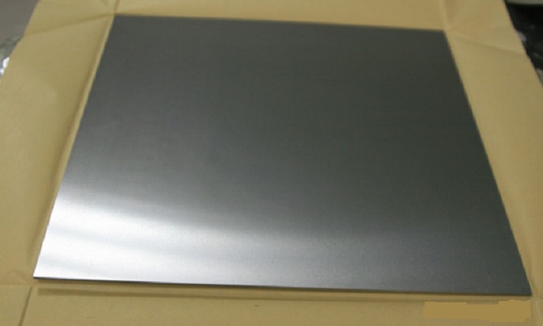
As a refractory metal with a very wide range of uses, molybdenum has excellent mechanical properties at high temperatures, low expansion, high thermal conductivity, and extremely high electrical conductivity. As a sputtering target, there are many combinations, such as pure molybdenum target, molybdenum titanium target, molybdenum tantalum target, and molybdenum alloy target (such as TZM plate).
The molybdenum sputtering target has the characteristics of high purity, high density, fine and uniform crystal grains, so as to obtain extremely high sputtering efficiency, uniform film thickness, and smooth etching surface during sputtering.
All targets of Advanced Refractory Metals (ARM) are specially designed to operate reliably during thin film deposition. The manufacturing process can ensure high purity, fine and uniform particles of the target material.
Conclusion
Thank you for reading our article and we hope it can help you have a better understanding of molybdenum sputtering targets for semiconductors. If you want to learn more about molybdenum or other refractory metals, we would like to advise you to visit Advanced Refractory Metals (ARM) for more information.
Headquartered in Lake Forest, California, USA, Advanced Refractory Metals (ARM) is a leading manufacturer & supplier of refractory metals & alloys across the world. It provides customers with high-quality refractory metals & alloys such as molybdenum, tantalum, rhenium, tungsten, titanium, and zirconium at a very competitive price.
REVIEWS
{{viewsNumber}}
Thought On "{{blogTitle}}"
{{item.name}}
{{item.created_at}}
{{item.content}}
LEVE A REPLY
Comment
Name
*
Email
*
{{item.children[0].name}}
{{item.children[0].created_at}}
{{item.children[0].content}}
{{item.name}}
{{item.created_at}}
{{item.content}}
More Replies
LEAVE A REPLY
Comment
*
Name
*
Email
*
SUBSCRIBE OUR NEWSLETTER
Your Name
*
Your Email
*
Success ! You're now subscribed
You've been successfully subscribed! Check your inbox soon for great emails from this sender.
Our Latest News
Tel : (949) 407-8904
Address : 1940 East Deere Avenue, Suite 100, Santa Ana, CA 92705, U. S. A
Metals

Useful Links
Featured Posts